


A plain-English primer on the machines, companies, and choke points behind AI.
Everybody’s talking about AI. Almost nobody can explain the thing it actually runs on. Ask a room of smart executives how a chip gets made, who makes the machines that make the chips, or why the whole world watches one company on one island, and you’ll get a lot of confident nodding and very few real answers.
That’s fine. You don’t need to be an engineer. But you do need a map. The AI economy isn’t magic software floating in the cloud. It is a physical industrial system built by a surprisingly small number of companies. Once you see how the pieces fit, the headlines stop being noise and start making sense.
We’ll walk through the ecosystem from the chip blueprint to the machines, materials and factories that build it, and finally to the memory, packaging and networks that turn those chips into AI. No math. No lab coat required.
Start Here: A Chip Is Just a Very Small City
A modern computer chip is a slab of silicon smaller than your fingernail containing billions of tiny switches called transistors. Each transistor can turn on or off. Those switches represent the ones and zeros behind computing. Put billions of them together and you can perform an extraordinary number of calculations very quickly.
When you hear ‘3-nanometer’ or ‘2-nanometer,’ think generation, not ruler. Those labels no longer describe one literal dimension on the chip. They identify increasingly advanced manufacturing technologies designed to pack more computing capability into a given area while improving performance and energy efficiency.

The Big Split: Who Designs vs. Who Builds
Here’s the single most important thing to understand about this industry: the company that designs a chip often does not manufacture it. Those are different businesses, run by different companies, frequently on different continents.
TSMC helped reshape the industry around the ‘foundry’ model: manufacture chips designed by customers without competing against those customers with its own branded processors. The flip side is the ‘fabless’ company, which designs chips but does not own the leading-edge factory that makes them. NVIDIA is the famous example. Apple, AMD, Qualcomm and Broadcom also rely heavily on foundries.
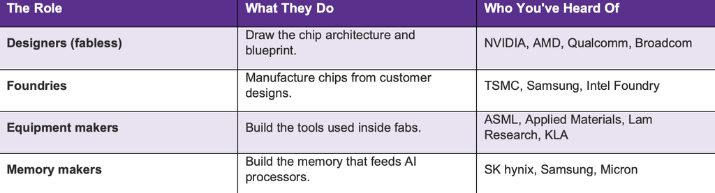
Keep that split in your head and half the confusing headlines suddenly make sense. A shortage of NVIDIA systems may originate in foundry capacity, HBM memory, advanced packaging or networking. Design and manufacturing are different links in the chain, and they can bind in different places.
The Most Important Machine You’ve Never Heard Of
Before a leading-edge chip can be built, its microscopic patterns must be printed onto a wafer. Lithography uses light to project extraordinarily tiny patterns onto a light-sensitive material covering the wafer. Other manufacturing steps then transfer those patterns into the layers that ultimately become the chip.
For the most advanced layers, manufacturers use extreme ultraviolet, or EUV, lithography. ASML of the Netherlands is the only commercial supplier of EUV lithography systems. These machines are among the most complex pieces of manufacturing equipment ever built and cost hundreds of millions of dollars at the high end.

But ASML does not make a chip by itself. A wafer can pass through hundreds of process steps. Applied Materials supplies equipment that deposits extremely thin layers of material. Lam Research is a leader in etch and deposition. KLA builds inspection and metrology systems that hunt for microscopic defects. The machines are an ecosystem too.
From Sand to Silicon: The Hidden Ingredients
Chips begin with silicon that is purified to extraordinary levels and formed into round wafers. But the wafer is only the starting surface. Modern fabs also consume photoresists, specialty gases, high-purity chemicals, metals and advanced substrates. Japan is particularly important in several of these material categories, alongside suppliers in the United States, Europe, Taiwan and South Korea.

The Most Complicated Factory on Earth
The chip factory is called a ‘fab,’ short for fabrication plant. A leading-edge fab can require investment measured in tens of billions of dollars and years of construction and qualification. Inside, contamination control is extreme because tiny defects can destroy devices measured in nanometers.
Getting a fab to produce good chips reliably is its own discipline, called ‘yield.’ A wafer contains many individual chips, and the economics improve dramatically when a larger share of them work. Yield comes from process knowledge, equipment tuning, materials control and thousands of incremental lessons learned over time.

How a Chip Becomes AI: Memory and Packaging
A powerful processor is only useful if it can get data fast enough. That’s where high-bandwidth memory, or HBM, comes in. HBM stacks multiple memory dies vertically and places them very close to the processor, creating an extremely wide, short pathway for data. Think of it as replacing a two-lane road to the GPU with a multilane expressway.
The leading HBM suppliers are SK hynix, Samsung and Micron. The concentration matters because a shortage of memory can leave an expensive accelerator waiting for data instead of computing.
Then comes advanced packaging. Packaging is no longer just the protective shell around a finished chip. It is increasingly the architecture that connects processors, HBM and other chiplets into one high-performance system. TSMC’s CoWoS family is a prominent example used for high-performance computing and AI.

The Next Bottleneck: Moving the Data
Once thousands of accelerators are installed in an AI cluster, another problem appears: they have to talk to one another. Networking determines how quickly data can move among GPUs, memory, switches, storage and racks. Companies such as NVIDIA, Broadcom, Marvell, Arista and Cisco sit in this layer of the stack.
Photonics is becoming more important as those data rates climb. Instead of moving every bit as an electrical signal through copper, optical links use light. Coherent and Lumentum supply important optical components, while Broadcom, Marvell, Cisco and others are pushing silicon photonics and co-packaged optics closer to the computing and switching silicon.
And underneath all of it are power and cooling. AI hardware can only scale as fast as data centers can secure electricity, transformers, backup power, cooling systems and grid connections. At that point the chip story becomes an infrastructure story.

The Whole Map, in One Read
Read this top to bottom and you have a practical map of the physical AI economy.
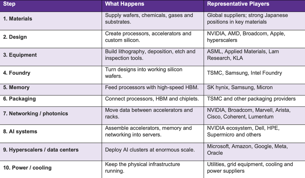
Notice the pattern: several critical layers are unusually concentrated. One EUV supplier. A small group of leading-edge foundries. Three major HBM suppliers. Specialized packaging and networking capacity. Concentration creates efficiency and extraordinary technical specialization, but it also creates choke points.
So Why Is Everyone Nervous About Taiwan?
Now the geopolitics makes sense. TSMC is the dominant manufacturer of leading-edge logic used across advanced computing, and Taiwan remains the center of its most advanced manufacturing footprint. That concentration gives governments and technology companies a powerful incentive to diversify capacity geographically.
TSMC is already expanding outside Taiwan. Its first Arizona fab entered high-volume production in late 2024, with additional Arizona fabs and advanced-packaging facilities planned. It is also expanding in Japan and Europe while continuing major leading-edge investment in Taiwan.
The important distinction is that capacity diversification does not instantly create capability diversification. Buildings can be replicated faster than ecosystems, skilled workforces, supplier networks and accumulated manufacturing know-how. Geographic diversification is happening, but the transition is measured in years, not quarters.
The Economic Lesson: The Advantage Is Synchronicity
The biggest lesson from the AI buildout is that AI is not one technology. It is a synchronized industrial system. A shortage of GPUs can constrain growth. Solve GPUs and HBM can become the constraint. Solve memory and packaging can bind. Then networking. Then power. Then cooling. Then capital.
That means the unit of competition is increasingly the system, not the individual chip. The winners will not necessarily be the companies with the best single component. Advantage increasingly comes from getting compute, memory, packaging, networking, power and capital to arrive at the same place at the same time.

The Bottom Line
The next time you read an AI headline, place it on the map. Is it a design story? A manufacturing story? A memory or packaging story? A networking story? A power story? Once you know where in the chain something is happening, you can judge whether it is noise, a temporary bottleneck or a structural shift.
You don’t need to build a chip. You need to understand how the physical AI economy fits together, where it is concentrated and where the bottleneck is moving next. Do that, and AI stops looking like magic software and starts looking like an industrial system you can read.
Want the forward-looking version of this story, where these choke points are moving and creating the next set of winners and losers? Read the companion piece, Chip Reset: Turning Bottlenecks into Breakthroughs.
Sources and Further Reading
This primer is a plain-language synthesis for general understanding, not investment advice. Key company and technical references used to verify the updated discussion include:
• TSMC 2025 Annual Report — Advanced process technology, CoWoS/3D integration, photonics and global manufacturing expansion. (investor.tsmc.com)
• Micron: High-Bandwidth Memory — HBM architecture, stacking, bandwidth and proximity to processors. (micron.com/products/memory/hbm)
• NVIDIA Networking — AI networking and data-center connectivity. (nvidia.com/en-us/networking)
• ASML: EUV Lithography — EUV lithography technology and systems. (asml.com/en/products/euv-lithography-systems)